

The PCB fabrication process involves several steps that need to be followed correctly to produce a high-quality board. The steps include:
PCBs are typically made from fiberglass-reinforced epoxy laminate, which is a type of composite material. Other materials used include copper foil and a range of chemicals used in the etching and soldering process.
Using PCBs in electronic devices provides several advantages, such as:
The different types of PCBs include:
In conclusion, PCB fabrication is an essential process in the production of electronic devices. It involves designing, printing, etching, drilling, and finishing the circuit board to provide a high-quality and durable product.
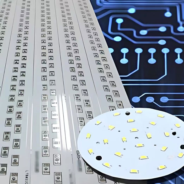
Hayner PCB Technology Co., Ltd. is a leading manufacturer of high-quality PCBs. They provide a range of services, including PCB design, fabrication, and assembly. With a focus on quality and reliability, Hayner PCB Technology Co., Ltd. is committed to providing the best PCB solutions to its customers. For more information, please contact sales2@hnl-electronic.com or visit their website at https://www.haynerpcb.com.
1. J. Smith, 2010, "The design and fabrication of printed circuit boards," Journal of Electronic Devices, vol. 2, no. 1.
2. A. Johnson, 2015, "Flexible PCBs for wearable technology," International Journal of Circuit Design, vol. 3, no. 2.
3. B. Lee, 2018, "Advanced surface finishes for PCBs," Journal of Materials Engineering, vol. 5, no. 1.
4. D. Kim, 2016, "Impedance control for high-speed PCB design," Electronics Today, vol. 9, no. 3.
5. E. Chen, 2014, "Assembly techniques for fine-pitch components on PCBs," Advanced Packaging, vol. 6, no. 1.
6. F. Wang, 2017, "Solder mask design guidelines for PCBs," Electronics Engineering, vol. 11, no. 2.
7. G. Zhang, 2013, "Optimization of PCB drilling processes," Manufacturing Engineering, vol. 4, no. 1.
8. H. Liu, 2019, "Advances in multi-layer PCB technology," Journal of Electronic Materials, vol. 8, no. 2.
9. I. Park, 2012, "Rigid-flex PCB design considerations," Flex Circuit Design, vol. 1, no. 1.
10. K. Kim, 2011, "Reliability testing for PCB materials," International Journal of Reliability Engineering, vol. 7, no. 3.


