


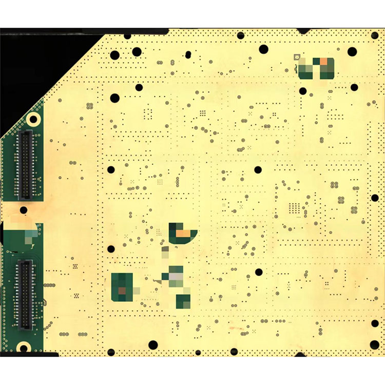
Hayner PCB 's main product - Heavy Copper PCB, a product proudly manufactured in China by a , a product proudly manufactured in China by a leading manufacturer and supplier in the electronics industry. This PCB meets the highest standards in the market, ensuring reliable and efficient power distribution. With its heavy copper design, it offers superior conductivity and durability, making it ideal for high-power applications. Despite its premium quality, we offer this PCB at a competitive price, ensuring value for money for our esteemed customers.
Usually PCBs are manufactured using copper thicknesses ranging from 1oz to 3oz. Heavy copper PCB is also known as thick copper PCB, in which there are 3 ounces (oz) of copper or more on the internal and external layers of aprinted circuit board. The circuit board with a copper thickness of more than 4 oz per square foot (ft2) is also categorized as a heavy copper PCB.

Heavy copper PCBs come with numerous benefits over standard PCBs.
Some PCBs are designed to carry higher current levels (amperage) by using wider traces. However, as power requirements increase, thicker copper is needed to transmit signals across the board.This is why heavy copper PCBs are used in high current designs.
The construction of a heavy copper circuit endows a board with benefits such as:
Improved thermal performance: Heavy copper PCBs can withstand repeated thermal cycles during manufacturing and assembly processes.
Increased current carrying capacity: Heavy copper PCBs offer better electrical conductivity and can handle higher current loads. Increasing the copper trace width can enhance the current carrying capacity, and thicker copper traces can handle even larger current loads.
Increased mechanical strength: Heavy copper PCBs enhance mechanical strength at connectors and plated-through holes, ensuring the board's structural integrity and making the electrical system more robust and resistant to voltage.
Excellent dissipation factor: Heavy copper PCBs are highly suitable for large power-loss components. These PCBs can prevent electrical systems from overheating and effectively dissipate heat.
Good conductor: Heavy copper PCBs are good conductors, making them useful in the production of electronic products. They help to connect various boards together, which can transmit currents.
Heavy copper PCBs are ideal for defense and military applications, medical devices, and many other areas.The demand for heavy copper PCBs is continuously increasing.
Military: Weapons control, radar, and monitoring systems.
Automotive industries: Rail track system and signal transmission system.
Power distribution: Excitation systems for power regulators, power grid switching systems, high power rectifiers, and overload relays.
Transportation: Power converters for railway systems, power line monitors, traction converters.
Industrial controls: Safety and signal systems, welding equipment, protection relays, surge protectors.
Renewable Systems: Power converters, energy storage, power grid back-up, hydroelectric power plants control panels
|
Specifications |
Capability |
|
HDI PCB Material |
FR-4, HI Tg, Rogers, Taconic, Argon etc. |
|
HDI PCB layer |
1-30 layer |
|
HDI PCB types |
single/double-sided, multi-layer |
|
Copper Thickness |
1-6oz |
|
Board Thickness |
S/D 0.2-0.7mm, Multi-layer:0.40-7.0mm |
|
Surface finish |
HASL,OSP,Immersion gold,Flash Gold Finger |
|
Min. Hole Size |
0.2mm mechanical drill |
|
4mil laser drill |
|
|
Min.Line Spacing / Min.Line Width |
6mil |
|
6mil |
|
|
Min. Solder Mask Bridge |
0.08mm |
|
Max. Production Size |
400x510mm |
|
Impedance control |
50Ω ±5Ω, 90Ω ±9Ω, 100Ω ±10Ω |
|
Aspect ratio |
15:1 |
|
Via Plugging Capability |
0.2-0.8mm |
|
PCB Standard |
IPC-II Standard |
|
Warp & Twist |
0.75% |
|
Certificate |
ISO9001.IATF16949.RoSH.UL. |
|
Quality Control |
X-ray, AOI Test, Function Test (100% Test) |
|
Delivery |
PCB 3-7 Days, PCBA 2-3 weeks |
Seven SMT production lines --10 millions points/day
Four THT production lines --- 0.50million points /day
Three Final assembly lines ----15,000pcs/day
One Aging room --------------2,000PCS/day
Three Spraying lines
Address
No. 15 Xinyuan Road, Wuqing Development Zone, Wuqing District, Tianjin, China
Tel


