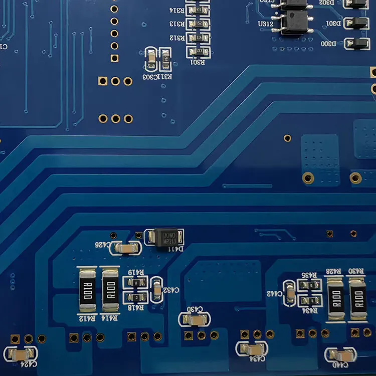
The production process of high frequency PCB involves several key steps, including material selection and preparation, lamination process, welding and assembly process, as well as specific design principles and strategies.

First of all, the materials used in high frequency PCB manufacturing have special electrical and mechanical performance requirements. The substrate material needs to have a low dielectric constant and dielectric loss to ensure the stability and reliability of signal transmission. The conductive layer needs to have good conductivity and corrosion resistance to ensure the reliability of signal transmission and connection. Auxiliary materials such as film materials and filling materials also need to be carefully selected and prepared to meet the requirements of high frequency PCB manufacturing.
The manufacturing of high frequency PCB mainly includes the steps of design, drawing making, etching, and laminating. First, the circuit design and layout planning are carried out according to the design requirements and signal transmission characteristics. Then, the PCB drawings are made to convert the circuit layout and connection lines into the circuit diagram on the drawings. Next, the circuit diagram on the drawings is transferred to the substrate through photolithography technology and etched to form a conductive layer. Finally, the laminating process attaches the protective layer and copper cladding layer to the conductive layer to protect the circuit and improve the mechanical strength.
The welding and assembly process of high-frequency PCBs is different from that of ordinary PCBs. Surface mount technology is widely used in the welding of high-frequency PCBs, and SMT components are accurately soldered to PCBs through methods such as hot air or reflow soldering. Manual soldering technology also occupies an important position in the assembly of high frequency PCBs, and plug-in components and connecting lines are connected through manual soldering. These welding and assembly processes require a high degree of precision and professional technology to ensure the performance and reliability of high-frequency PCBs.
In terms of design, high frequency circuit design requires a series of special design principles and strategies to ensure signal quality and system reliability. This includes considering challenges such as transmission line effects, signal integrity issues, and electromagnetic interference (EMI). High frequency signal lines should be as short and straight as possible, with fewer corners to reduce the inductance of the signal path and reduce transmission delays. Multilayer board design helps isolate different signals and reduce cross-interference. High-frequency signals are usually arranged on the inner layer and as close to the ground plane as possible, using the ground plane as a return path to enhance the shielding effect of the signal.
In summary, the production of high frequency PCB involves fine operations and professional processing in multiple links, from material selection, design layout, welding assembly to wiring strategy, to ensure the stable transmission of high frequency signals and the reliability of the system.
