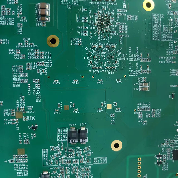
One of the key differences between Large Format PCBs and standard PCBs is their size. Large Format PCBs can be up to 4 feet by 8 feet and can handle higher power loads. Another difference is the number of layers that can be included in the PCB. Large Format PCBs can have more than 40 layers, whereas standard PCBs typically have fewer than 10 layers. Large Format PCBs also require specialized manufacturing equipment and processes, which can increase their cost compared to standard PCBs.
Large Format PCBs offer several advantages over standard PCBs, including increased design flexibility, improved signal integrity, and enhanced power handling capabilities. These PCBs can accommodate larger components and more complex circuit designs, making them ideal for use in high-performance applications. Large Format PCBs also have a lower risk of failure in high-current applications, which can result in improved reliability and reduced maintenance costs.
Large Format PCBs are used in a variety of applications that require a higher power handling capability or more space for components. These applications include power electronics, telecommunications, medical devices, aerospace, and automotive electronics. Large Format PCBs are also used in applications that require high-density interconnects, such as data centers and server farms.
Large Format PCBs present several challenges for designers and manufacturers, including increased cost, longer lead times, and higher manufacturing complexity. The large size of these PCBs requires specialized manufacturing equipment and processes, which can drive up the cost and lead time. Additionally, the larger size of these PCBs can make them more difficult to handle and inspect during the manufacturing process.
In conclusion, Large Format PCBs offer several advantages over standard PCBs, including increased design flexibility, improved signal integrity, and enhanced power handling capabilities. These PCBs are commonly used in high-performance applications, such as power electronics, telecommunications, and medical devices. However, they also present several challenges for designers and manufacturers, including increased cost, longer lead times, and higher manufacturing complexity.
Hayner PCB Technology Co., Ltd. is a leading manufacturer of Large Format PCBs. With over 20 years of experience in the industry, we have the expertise and manufacturing capabilities to produce high-quality Large Format PCBs for a variety of applications. Visit our website at https://www.haynerpcb.com to learn more about our products and services. For sales inquiries, please contact us at sales2@hnl-electronic.com.
1. Kim, J., Kim, S., & Lee, K. (2018). Thermal analysis of large format PCBs using integrated thermoelectric modules. Proceedings of the 18th IEEE/ACM International Conference on Thermal, Mechanical and Multi-Physics Simulation and Experiments in Microelectronics and Microsystems.
2. Zhang, G., Chen, Y., & Li, Y. (2017). Design and analysis of a high-power density interleaved buck converter using Large Format PCBs. IEEE Transactions on Power Electronics, 32(10), 7914-7924.
3. Roh, S., Kwon, H., & Park, Y. (2016). Design and implementation of a large-format LED matrix display system based on modular PCBs. International Journal of Software Engineering and Its Applications, 10(12), 273-282.
4. Huang, H., Yuan, J., & Chen, Y. (2015). Large format PCB design for automotive inverter application. 2015 IEEE International Conference on Electrical Systems for Aircraft, Railway, Ship Propulsion and Road Vehicles (ESARS).
5. Shi, W., Zhang, L., & Xiong, X. (2014). Analysis of signal integrity in Large Format PCB design. Journal of Semiconductors, 35(11), 1-7.
6. Aung, Y., Shin, J., & Kwon, Y. (2013). Mitigation of electromagnetic interference in Large Format PCBs using a split power plane. Progress in Electromagnetics Research, 142, 141-149.
7. Chi, W., Wang, L., & Li, P. (2012). Design and realization of Large Format PCB-based high-speed data acquisition system. Chinese Journal of Scientific Instrument, 33(11), 2667-2672.
8. Luo, H., Li, B., & Zhang, X. (2011). Design and implementation of a Large Format PCB-based power distribution system for server farms. 2011 IEEE International Conference on Automation and Logistics.
9. Wang, H., Luo, Z., & Liu, Q. (2010). Design and implementation of a Large Format PCB-based solar inverter. Proceedings of the 2010 IEEE International Conference on Intelligent Computing and Integrated Systems.
10. Lai, J., Lin, Y., & Su, Y. (2009). Thermal analysis of Large Format PCBs with high-power LEDs. IEEE Transactions on Components and Packaging Technologies, 32(3), 684-693.
TradeManager
Skype
VKontakte
